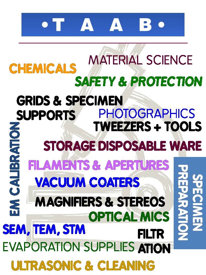
Materiale per SEM e TEM
Consumabili ed accessori per microscopia elettronica.
Ecco tutte le sezioni scaricabili del catalogo TAAB:
- Grids and Support Films
- EM Filaments & Apertures
- EM Calibration
- Filtration
- Specimen Preparation
- Tweezer
- Vacuum Coaters
- Evaporation Supplies, Oils & Greases
- Material Science
- SEM, TEM, STM Supplies
- Optical Microscopy
- Microtomy and Histology
- Water Chillers
- Ultrasonic and Cleaning Supplies
- Magnifiers and Stereoscopes
- Storage and Disposable Ware
- Photographic Supplies
- Safety and Protection
- Chemicals
- Chemical Listing
- Index
Tutto 12 /ALD 2 /Alta temperatura e Atmosfera controllata 0 /Analitici 0 /Assottigliatori Ionici 0 /Attivazione superficiale e Plasma Cleaning 0 /BLACK MAGIC per deposizione grafene e CNT 3 /Caratterizzazione ottica 0 /Catodoluminescenza 0 /Catodoluminescenza/EBIC 0 /Critical Point Driers 0 /Cross Section Prep. Kit 0 /Cryo Plunge 0 /CVD 0 /Dimple Grinder 0 /Disc Grinder 0 /Ellissometri laser 0 /Ellissometri spettroscopici 0 /Etching e Coating Systems 0 /Evaporatori e Sputter Coaters 0 /Forni & Stufe 0 /GIF Hardware e Software 0 /Glove box, Isolatori e Flow Box 0 /In Aria 0 /In Vuoto 0 /Measure Samples 0 /Microdispensing e inkjet printing 1 /Micromanipolatori 0 /Microscopi a Forza Atomica 0 /Misura 4 punte 0 /Misura effetto Hall a T ambiente 0 /MOCVD 2 /Multispecimen 0 /NanoIR 0 /NanoTA 0 /Nanotech 5 /News 0 /PECVD – ICPECVD 2 /Per SEM 0 /Per TEM 0 /Plasma Cleaners 0 /Portacampioni 0 /Process Samples 0 /Raffreddanti e Cryo-Transfer 0 /Riflettometri 0 /Riflettometri e Ellissometri 0 /Riscaldanti 0 /Sample Preparation 0 /SEM 0 /Serial Block Imaging 0 /Simulatori Solari - IQE/EQE 0 /Sistemi CVD e ALD 1 /Sistemi nanoIR e nanoTA 0 /Sistemi per etching reattivo 1 /Sistemi PVD 0 /Spettrometri 0 /Stages Dedicati 0 /SThM 0 /Straining Holders 0 /Telecamere 0 /TEM 0 /Tomografici 0 /Ultrasonic Cutter 0 /Vacuum Transfer 0
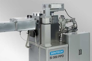
PECVD loadlock system SI 500 PPD
The flexible PECVD system SI 500 PPD features a variety of standard plasma deposition processes. SiO2, SiNx, SiOxNy, and a-Si are deposited with capacitively coupled plasma.
19 Febbraio, 2016/da Demo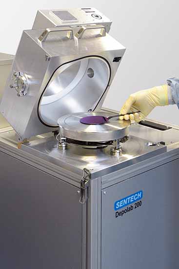
PECVD direct loading system Depolab 200
The PECVD system Depolab 200 combines cost effective direct loading and parallel plate plasma source in a basic, compact design. The easy to use direct loading system enables user-friendly batch processing (with carrier or direct loading onto the substrate electrode). The clever PECVD system can be upgraded for enhanced performance on demand
19 Febbraio, 2016/da DemoQXP-8300 ALD System
Atomic layer deposition is a process for manufacturing ultrathin films for semiconductor components and future non-semiconductor applications
23 Febbraio, 2016/da DemoQXP-8300 ALD System
Atomic layer deposition is a process for manufacturing ultrathin films for semiconductor components and future non-semiconductor applications
23 Febbraio, 2016/da DemoQXP-8300 NVM
The Highest Deposition Rate with Excellent Composition Control and Conformality
23 Febbraio, 2016/da Demo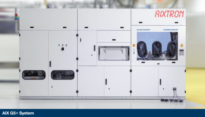
MOCVD – Planetary Reactor
The Planetary Reactor is based on the principle of a horizontal laminar flow reactor. The laminar flow principle ensures extremely precise transitions between different materials, and an unparalleled control over the deposition rates for films that are only a few atoms thick
23 Febbraio, 2016/da Demo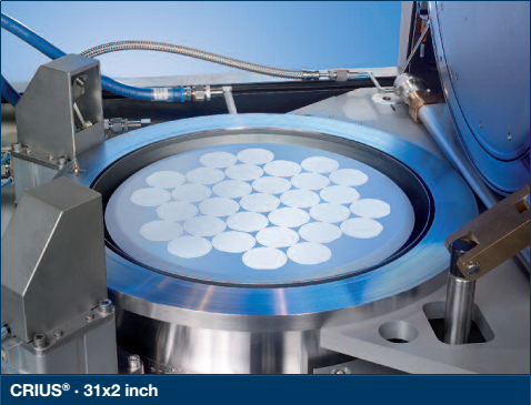
MOCVD – Close Coupled Showerhead
23 Febbraio, 2016/da Demo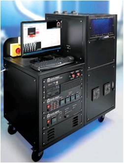
Black Magic 2″ – R&D
Applying this methodology, the deposition of thin films takes place by means of chemical reactions, in which the wafers are exposed to a gas mixture that reacts on the wafer surface. The process can also be plasma-enhanced
24 Febbraio, 2016/da Demo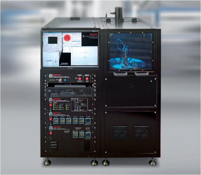
BLACK MAGIC PRO
Wafer-scale Deposition of Carbon Nanotubes and Graphene
BM Pro…
24 Febbraio, 2016/da DemoBM Pro…
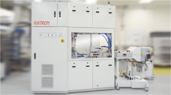
BLACK MAGIC 300
24 Febbraio, 2016/da Demo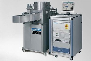
ICP-RIE plasma etcher SI 500
The high end plasma etching system SI 500 uses an inductively coupled plasma with low ion energy for low damage etching and nano structuring. Repeatable and stable plasma etching conditions are ensured by dynamic temperature control over a wide temperature range. Cryogenic and room temperature, gas chopping processes are applied for deep reactive plasma etching (Si, III-V semiconductors, MEMS)
24 Febbraio, 2016/da Demo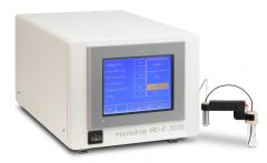
MD-E-3000
Small volume handling with microdrop dispensing system
24 Febbraio, 2016/da Demo